-
全國咨詢服務(wù)熱線:
0592-7199126

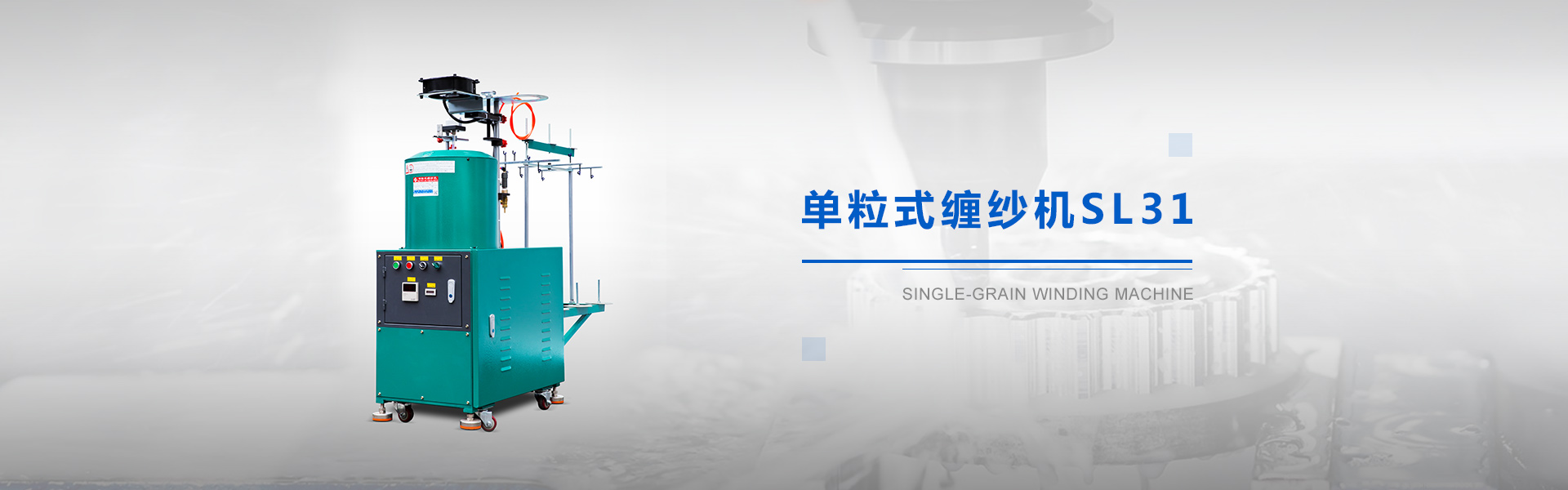
熱門搜索關(guān)鍵詞: 糊料攪拌桶 單粒式纏紗機(jī) 彈跳測試儀 定壓充氣機(jī) 油壓切膠機(jī)
多行業(yè)都在使用我們的產(chǎn)品Innovative manufacturing, change production, the product will be more refined and better quality higher, to create the industry eagle brand


 關(guān)注省力機(jī)械抖音號